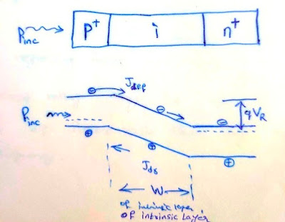
It is a junction photo diode.
Basic principle :- The diode is operated under reverse biased condition. Under photo excitation , photons are absorbed mainly in depletion region and also in neutral region , particularly on top where light is incident. the absorbed photons create e-h pairs
They give rise to photo current , the magnitude of which depends on quantum efficiency.
so photo excitation is therefore detected as an increase in reverse biased current of a junction photo diode.
Large depletion layer may increase no.of e-h pairs generated but it consequently increases response time of diode degrading its high speed performance.
Pin diodes have no internal gain but can have very large band widths.
Since dark current in a reverse biased junction is very small , pin diode is more sensitive device than a photo conductor.
